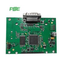
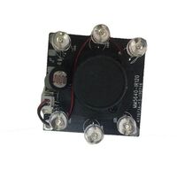
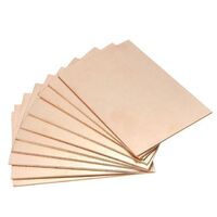
Professional One Stop Service Double Sided HDI Mini GPS Tracker PCB Design
- $4.09 / 1 - 99 pieces
$3.01 / 100 - 999 pieces
$1.93 / >=1000 pieces - 1 piece
- Shenzhen Ilinkglobe Co., Ltd.
- Guangdong, China
- Mr Wang Michael
PRODUCT DETAIL
| Original Equipment Manufacturer: | acceptable | type: | heavy copper pcb |
| Craft: | Reflow and Soldering | minute. Hole size: | 0.25mm |
| shape: | rectangle, circle, irregular | minute. Line spacing: | 0.075mm |
| port: | Shenzhen Yantian Port | Floor: | up to 40 floors |
| brand: | Link Earth | Certification: | ISO9001 |
| Minimum PCB Thickness: | 0.1mm | place of origin; place of origin: | Guangdong, China |
| Features: | CAD+PCB+Components+SMT | sample: | 1 |
| Copper Thickness: | 0.2mm | Board size: | 50*50mm-910mm*600mm |
| model: | ZLKX-TX-002 | payment terms: | L/C,Western Union,D/P,D/A,T/T,MoneyGram |
| application: | industrial control | Surface treatment: | Spray tin, lead-free spray tin |
| minute. Line width: | 0.075mm | Packaging Preview: | |
| Maximum printed circuit board size: | 910mm*600mm | Supply capacity: | 800 pieces per day |
| Plate thickness: | 1.2mm | Substrate: | FR-4, High Tg FR4, High CTI FR4 |
Product Description
product name | PCB PCBA Manufacturer |
application | Telecom, medical, industrial control, new energy, automobile, robot, 5G server, drone |
boring | FR-4, high Tg FR4, high CTI FR4, halogen-free FR4, copper aluminum plate |
flexible | Rogers, Arlon, Taconic, Nelco, Isola |
PCB layer | 1-40 layers |
PCB shape | Rectangle, Square, Circle, Irregular |
Board size | 50*50mm-910mm*600mm |
PCB thickness | 0.1mm-8mm |
Maximum finished copper thickness (inside and outside) | 120 oz |
Minimum base copper | 1/3 ounce |
Minimum drilling diameter | 0.1mm |
Minimum drilling tolerance | +/-2 million |
Minimum layer tolerance | +/-3 million |
Minimum line width/spacing | 3 million/3 million |
Minimum pitch (hole to inner or outer conductor) | 6000000 |
Minimum BGA Diameter | 800w |
Human Development Index | 1-3steps Anylayer |
surface treatment | HASL, lead-free HASL, ENIG, Ni/Au plating, gold finger, immersion silver/tin, OSP, ENIPG |
Manufacturer Services
Project Development Services
ILINKGLOBE provides product development services according to customers' specifications. If the project feasibility assessment is passed, the overall solution including software and hardware will be output. After the sample is made and tested, it will be further provided to the customer for verification or program modification. Finally, according to the needs of customers, it is determined to end the research and development program, or to continue the production of mass products.
The following files are required for project development:
1: Detailed function description
2: Description of technical parameters
3: Design cycle requirements
4: Batch cost requirements
1: Detailed function description
2: Description of technical parameters
3: Design cycle requirements
4: Batch cost requirements
PCB Design Services
ILINKGLOBE provides PCB design services according to customers' specifications. Customer provides DSN/SCHSchematic file and PCB package library file, or the corresponding device DataSheet. The customer needs to provide the PCB board structure file in DXF format, the structure restriction description, the electrical design description and other matters needing attention. After the project starts, our engineers will conduct DRC inspection on electrical design requirements such as schematic diagram and structural inspection. If there is a problem, the EQ record will be fed back to the customer as soon as possible. During the project design process, the daily work progress file of our engineers is sent to the clientconfirm. Customers can see the status of the design every day, and can find and deal with problems in a timely manner. After the design of Pcb Layout is completed, our engineers will conduct mutual inspection, including DFM inspection, QA inspection and EMC inspection. After the customer confirms OK, we will issue production documents such as GERBER. After the customer confirms OK, our engineers will output ASM assembly files, SMT patch files, original PCB design files, GERBER files, EQ engineering communication records, etc.
The following files are required for PCB design:
1: Schematic diagram of DSN/SCH format
2: PCB footprint
3: Package library file/main device data sheet
4: Outline structure drawing/DXF format/DWG format
5: Electrical design requirements such as layout/wiring/timing/frequency/speed/current
6: Reference board/PCB or BRD format
1: Schematic diagram of DSN/SCH format
2: PCB footprint
3: Package library file/main device data sheet
4: Outline structure drawing/DXF format/DWG format
5: Electrical design requirements such as layout/wiring/timing/frequency/speed/current
6: Reference board/PCB or BRD format
PCB Manufacturing Services
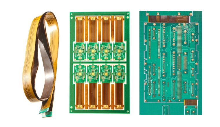
ILINKGLOBE provides PCB production services. We can make 1-40 layers rigid, 1-8 layers flex to 2-12 layers rigid-flex PCBs. Materials include standard FR-4, high Tg FR-4, halogen-free FR-4, copper aluminum plate, polyimide, PTFE, high-speed and high-frequency, etc.
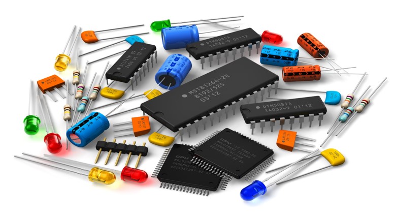
Parts Purchasing Service
ILINKGLOBE provides component procurement services. Components are purchased from reliable distributors such as Digikey, Mouser, Arrow, Avnet. After 10 years of experience, the quality of all components can be guaranteed.
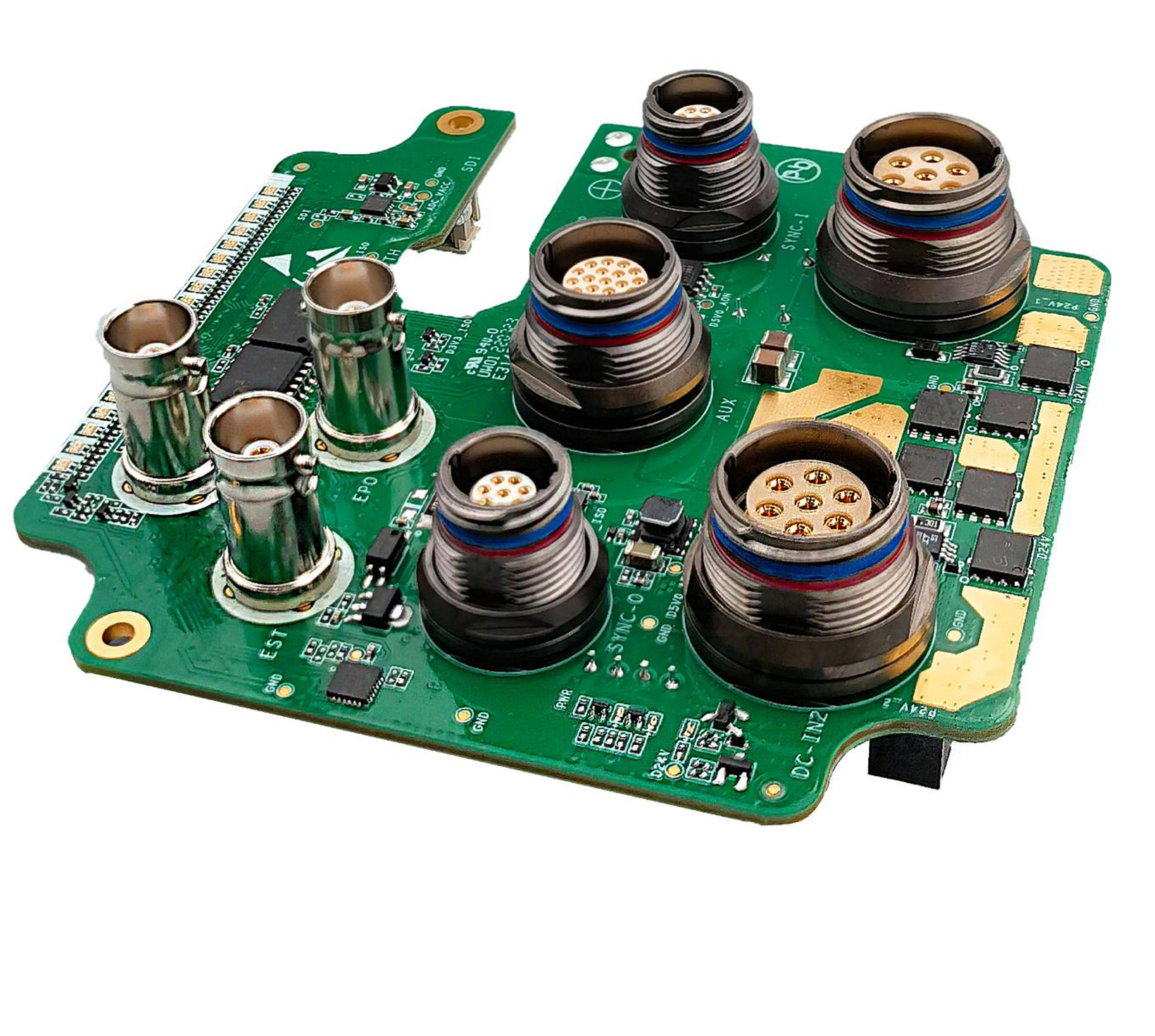
PCB Assembly Services
ILINKGLOBE provides PCB assembly services from prototype to mass production. Components range from 01005, BGA, LGA, QFN to DIP through hole. SPI, AOI, FA and X-Ray are all equipped to ensure quality. Both SMT formwork and cable assembly services can be provided.

programming and testing
ILINKGLOBE provides programming and functional testing services. Equipped with SPI FLASH programmer using Type-C communication interface and ISP/ATE multiplexing interface, which can be used for various SPI NOR FLASH, I2C/Micro Wire and other EEPROMs. Once detailed test instructions and documentation have been received, functional testing can be performed.
Application field

VIEW MORE
YOU MAY LIKE


