
Various models of OEM PCB assembly factory, PCBA contract manufacturer, PCBA board APP service
- $3.00 / 8 - 14 pieces
$1.00 / >=15 pieces - 8 pieces
- Guangzhou E-sun Technology Co.,Ltd.
- Guangdong, China
- Mr Ethan Lau
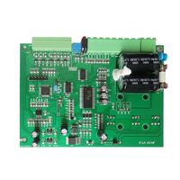
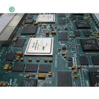
PRODUCT DETAIL
| payment terms: | L/C, Western Union, D/P, D/A, T/T, MoneyGram | Plate thickness: | 0.07-0.5MM |
| Minute Hole Size: | 0.1MM | Package preview: | |
| Design Manufacturer: | Yes | Supply capacity: | 100000 pieces per month |
| model: | Yisheng Daikin circuit board | type: | HDF |
| Copper thickness: | 1oz / 1/2oz/ 1/3oz, 1OZ | Minute line width: | 0.04MM |
| Surface treatment: | HASL / OSP / ENIG / Immersion Silver / Tin / Nickel, ENIG | Minute line spacing: | 0.04MM |
| Substrate: | polyimide/polyester | port: | Guangzhou Whampoa |
| Packaging Details: | carton; | Plate thickness: | 0.6mm |
| PCB samples available: | PCB and PCBA samples available | MOQ: | 10 |
| Material: | FR-4 and polyimide | Origin: | Guangdong, China |
| chip: | Yes | brand: | Yi Shun |
| Layers: | 2 layer | Board Dimensions: | 2.5kg/500pcs |

layers | 1-18 floors | Material | FR-4,FR2.Taconic,Rogers, CEM-1 CEM-3,ceramic , corcery Metal-backed Laminate | ||
surface treatment | HASL(LF), Gold Plating, Electroless Nickel Immersion Gold, Immersion Tin, OSP(Entek) | Veneer Thickness | 0.2mm-6.00 mm (8 million-126 million) | ||
copper thickness | 1/2 oz minimum; 12 oz maximum | Solder mask | Green/Black/White/Red/Blue/Yellow | ||
Minimum Trace Width and Line Spacing | 0.075mm/0.1mm(3mil/4mil) | CNC drilling minimum aperture | 0.1 mm (4 million) | ||
Punching minimum aperture | 0.9 mm (35 million) | Maximum panel size | 610mm*508mm | ||
hole position | +/-0.075 mm (3 million) CNC drilled holes | Conductor Width (W) | 0.05mm (2mil) or; +/-20% original work | ||
Aperture (H) | PTH L:+/-0.075mm(3mil); Non-PTH L:+/-0.05mm(2mil) | Profile Tolerance | 0.125 mm (5 million) CNC wiring; +/-0.15mm(6mil) stamping | ||
twist and twist | 0.70% | Insulation resistance | 10Kohm-20Mohm | ||
Conductivity | <50 ohms | Test voltage | 10-300V | ||
panel size | 110×100mm (minimum); 660×600mm (maximum) | layers of dislocation | 4 layers: 0.15mm (6mil) max; 6 layers: 0.25mm (10mil) max | ||
The minimum distance from hole edge to inner layer circuit pqttern | 0.25mm (tens of millions) | The minimum distance between the outer lines of the inner circuit board | 0.25mm (tens of millions) | ||
different impedance | +-/10% | Impedance control | +/-10% | ||
Plate Thickness Tolerance | 4 layers: +/-0.13mm (5mil); 6 layers: +/-0.15mm (6mil) | ||||


VIEW MORE
YOU MAY LIKE


Other Products
-
 China factory manufacture pcb rigid flex board for mobile phone camera pcb x ray machine$1.00 - $3.00 / piece